

THIN FILM DEPOSITION METHODS EXPLAINED
Thin film deposition is a critical process in modern electronics, energy systems and optical technologies. By depositing controlled material layers onto a substrate, manufacturers create conductive, optical and protective coatings with precise thickness and functional properties.
This guide explains the main thin film deposition methods, including PVD, sputtering and vacuum-based processes.

WHAT IS THIN FILM DEPOSITION?
Thin film deposition refers to the process of applying a very thin layer of material, typically ranging from nanometers to micrometers, onto a substrate surface. These films are used to modify electrical conductivity, optical transmission, mechanical durability or chemical resistance.
Thin films are essential in:
Semiconductor devices
Solar cells
Display technologies
Optical coatings
Transparent conductive layers
MAIN THIN FILM DEPOSITION TECHNIQUES
Physical Vapor Deposition (PVD)
A vacuum-based process where solid material is vaporized and condensed onto a substrate surface.
Common PVD methods include:
Sputtering
Thermal evaporation
Electron beam evaporation
Sputtering Deposition
A widely used PVD technique where energetic ions bombard a target material, ejecting atoms that deposit as a thin film.
Sputtering is particularly suitable for:
ITO coatings
Transparent conductive films
Semiconductor layers
Chemical Vapor Deposition (CVD)
A chemical process where gaseous precursors react at the substrate surface to form a solid thin film.
Often used for:
Semiconductor manufacturing
Hard coatings
Protective layers
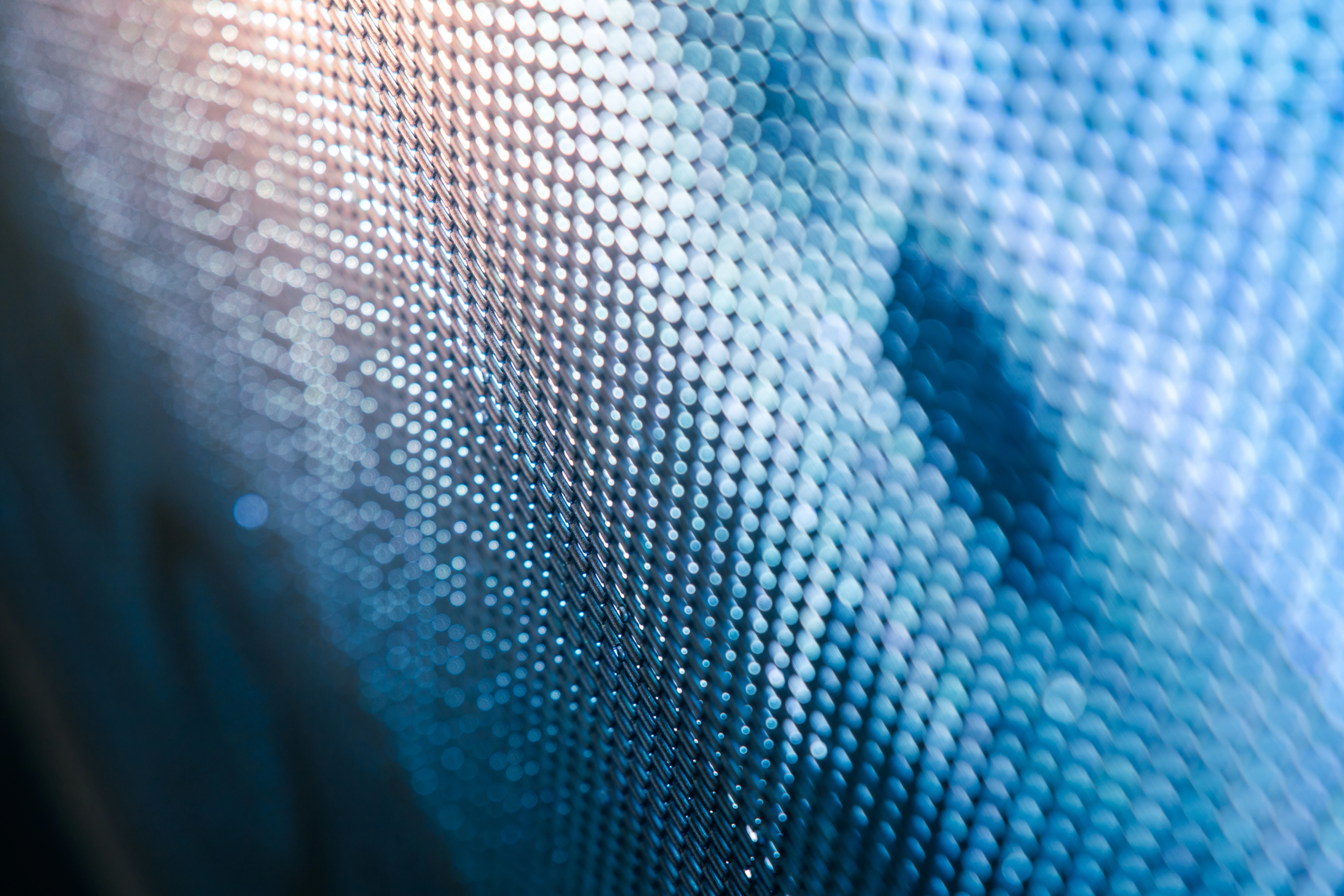
VACUUM DEPOSITION METHODS
Many thin film processes operate under vacuum conditions to ensure high material purity and controlled film growth. By reducing pressure inside the chamber, contamination is minimized and material transfer from source to substrate can be precisely controlled.
In processes such as sputtering, the vacuum environment enables stable plasma formation and uniform layer deposition. This level of control supports consistent electrical and optical performance across research and industrial applications.

Vacuum chamber
Target material
Plasma generation
Film growth

WHY SPUTTERING IS WIDELY USED FOR ITO THIN FILMS
ITO thin films are most commonly deposited using magnetron sputtering due to the high level of process control it provides. The technique enables precise thickness regulation and stable film composition, which are critical for achieving consistent electrical conductivity and optical transparency.
Sputtering also supports uniform layer formation across large substrate areas, making it suitable for both research environments and industrial scale production. Its reproducibility and compatibility with controlled vacuum conditions allow manufacturers to tailor film properties to demanding applications such as displays, touch panels and photovoltaic systems.
APPLICATIONS OF THIN FILM DEPOSITION
Thin film deposition technologies enable precise material layers that define the electrical, optical and protective performance of modern devices. The ability to control thickness, composition and uniformity makes these processes essential across multiple high performance industries.
Thin conductive and transparent layers are deposited onto glass or polymer substrates to create electrodes for LCD, OLED and capacitive touch systems. Uniform thickness and stable sheet resistance are critical for display clarity and responsiveness.
Transparent conductive layers are applied to photovoltaic substrates to balance light transmission with electrical conductivity. Controlled deposition improves efficiency, stability and long term performance in solar modules.
Thin films regulate charge transport and light emission efficiency in advanced lighting technologies. Precise deposition ensures consistent optical output and reliable device performance.
Vacuum deposited layers enhance reflection control, durability and surface functionality in optical components, architectural glass and industrial equipment.
Thin film processes are fundamental in integrated circuits, sensors and microelectronic components where nanometer-scale precision determines device functionality.
FAQ ABOUT THIN FILM DEPOSITION
TAILORED ITO SOLUTIONS FOR THIN FILM DEPOSITION
Whether you are developing a new coating process or scaling up industrial production, our technical team can help specify the right ITO material for your thin film application.