THIN FILM DEPOSITION MATERIALS

SPUTTERING TARGETS FOR THIN FILM DEPOSITION

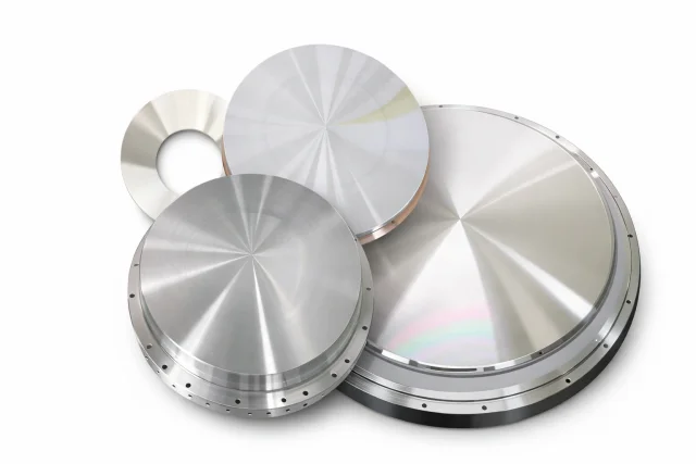
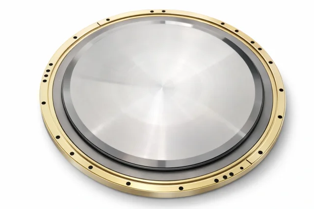
High purity sputtering targets engineered for controlled thin film deposition in semiconductor and advanced electronics manufacturing. Available for demanding PVD processes with dimensions adapted to specific deposition equipment and production requirements.

SPUTTERING TARGETS

HIGH PURITY TARGETS FOR PVD SPUTTERING

Sputtering targets provide the source material used to create functional thin films through physical vapor deposition (PVD). During the sputtering process, atoms are released from the target surface and deposited onto a substrate, enabling controlled formation of metallic layers with defined electrical and functional properties.

Material purity and target consistency are important factors in achieving stable deposition conditions and repeatable film performance. High purity materials help limit unwanted impurities, while controlled target properties support uniform sputtering behavior across semiconductor and advanced coating processes.

Target dimensions and material specifications can be adapted to different deposition systems and process requirements, supporting applications from development and testing to industrial-scale thin film production.


SPUTTERING TARGET APPLICATIONS

Sputtering targets are widely used in semiconductor and electronics manufacturing where controlled deposition of thin metallic films is required. Different target materials provide specific electrical, structural and functional properties depending on the intended application.

The appropriate target material and configuration depend on the substrate, deposition equipment and required film characteristics. Consistent target quality helps maintain controlled deposition conditions and reliable thin film performance across both development and industrial manufacturing.

Semiconductor Manufacturing

Thin metallic layers for wafer processing and semiconductor device fabrication.

Electronic Components

Conductive and functional coatings used in advanced electronic devices.

Wafer Processing

Controlled metal deposition for demanding wafer-scale manufacturing processes.

Thin Film Coatings

Metallic layers engineered for specific electrical and functional requirements.